Compiled code always have scalar instruction. Here is a thread binary that has only scalar instruction on it run as many copies as many threads you want. All the instructions have different program counter
GPU execute hardware threads scalar instructions. GPU cores detect when different hardware threads executing same instruction, and implements simultaneous execution of upto SIMD-width threads using SIMD (Single Instruction, Multiple Data) ALUs.
Let's see how V100 works.
NVIDIA V100 (Volta Architecture)
The 32-wide SIMD (Single Instruction, Multiple Data) operations of NVIDIA V100 GPUs architecture:
- SIMD Width: The V100 architecture uses a 32-wide SIMD for each warp, meaning each warp can process 32 threads simultaneously.
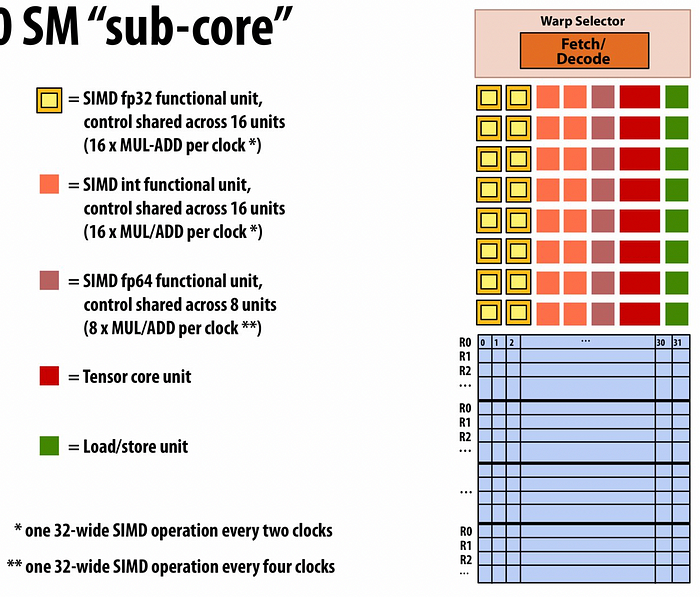
- CUDA Cores: Each Streaming Multiprocessor (SM) in V100 contains 64 FP32 CUDA cores, or each sub-core contains 64/4 = 16 FP32 CUDA cores(check yellow below).
- Tensor Cores: V100 introduced Tensor Cores designed for deep learning tasks, capable of performing mixed-precision matrix multiply-and-accumulate calculations.
- Precision: V100 supports FP32, FP64, and INT8 precision, with a significant focus on high-precision calculations.

stanford cs149 lecture 3 — instruction
In this image the instruction 6 is not consistent with other instructions so masked off.

stanford cs149 lecture — V100 1 SM's sub-core (4 per SM)

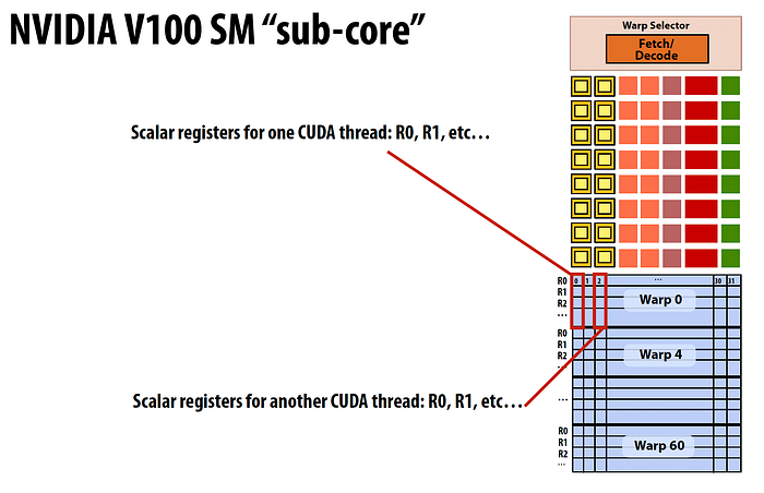
cs149 Stanford —Nvidia V100 — scalar register for 32 threads in single warp
Each sub-core within an SM has 64 kilobytes of register file storage available. This storage is used by the threads assigned to that sub-core to hold variables and intermediate results during computation.
For example:
cs148 Stanford. — match the color scheme
1 Warp can process upto 32 threads. The threads in a Warp is processed in SIMD manner.
However, there are 16 SMDI FP32 functional units (yellow ones), this means 1 Warp can process 16 FP32 SMDI functional units in 2 clock cycles.
16 ALU( yellow) x 2 clock cycles = 32 threads in warp.
16 SMDI int 32 (red ones) functional units, this means 1 Warp can process 16 SMDI int functional units in 2 clock cycles.
16 ALU( red ones in the image ) x 2 clock cycles = 32 threads in warp.
8 SMDI FP64 functional units, this means 1 Warp can process 8 SMDI FP64 functional units in 4 clock cycles.
8 ALU( brown ones in the image ) x 4 clock cycles = 32 threads in warp.
So in the above example, each instruction is run by all 32 threads. However, there are 16 ALUs( count yellow ), so running the instruction for entire 32 threads in the warp, it will take 2 clock cycles.
If 32 threads do not share the same instructions, then the performance is impacted.

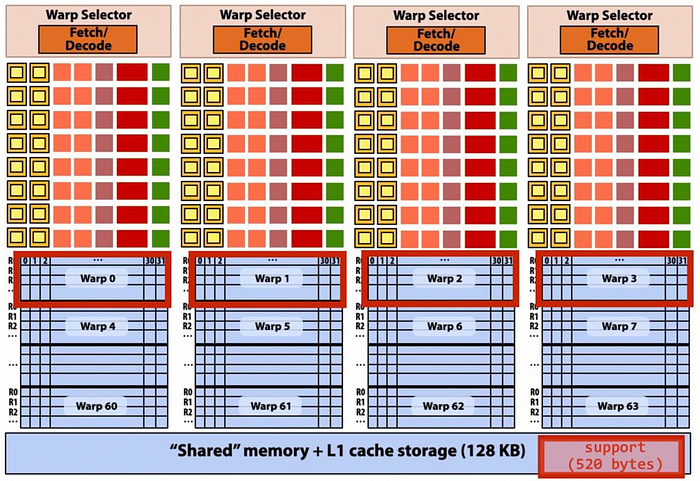
cs149 Stanford. — 1 SM unit containing 4 subcores.
For Nvidia V100, 1 SM has 4 sub-cores. There are 64KB registers/ sub-core.
1 SM 4 sub-core x 64KB/sub-core = 256KB registers per SM.
- For instance, if each thread in a warp uses 64 registers, and each register is 32 bits (4 bytes),
- then:
- Register usage per thread=64×4 bytes=256 bytes
- Register usage per warp=256 bytes×32 threads=8,192 bytes=8 KB
- Therefore, if a sub-core has 64 KB of registers, it can support a maximum of:
- 64 KB/8 KB=8 warps
- 8 KB x 8 warps before running out of register 64 KB space.
Lets go through the Cuda code block:

standard cude code
THREADS_PER_BLK = 128
128 threads per block /32 threads per warp = 4, 4 warps per SM or 1 warp per sub-core (there 8 warp per sub-core)
so the convolve function thread block is executed by 128 threads or by 4 warps.

Each sub-core runs next instruction for the CUDA threads in the warp (this instruction may apply to all or a subset of the CUDA threads in a warp depending on divergence.
so 128 threads per block and 4bytes per threads,
shared block has 128 threads + 2 threads (why?).
so 128threads x4 bytes = 512, 2 threads x 4bytes , 512+8=520 bytes (red one in the shared memory)
V100 has 80 SMs

Nvidia V100 80 SMs
V100 geometry
Clock Speed and Streaming Multiprocessors (SMs)
- 1.245 GHz Clock: This refers to the operating frequency of the V100 GPU. The clock speed determines how many cycles per second the GPU can execute, which directly impacts its performance.
- 80 SM Cores per Chip: The V100 GPU contains 80 Streaming Multiprocessors (SMs). Each SM is a unit within the GPU that contains multiple cores (4 sub-cores as discussed) for parallel processing.
Floating point (FP) ALUs and Performance
There are 16 single-precision floating-point (FP32) ALU (check the yellow ALUs in the picture)
80 (SM) x 4 (4 sub-cores) x 16 (MUL-ADD ALUs/clock) = 5,120 FP32 MUL-ADD ALUs
each FP32 MUL-ADD ALUs is 2 FLOPS
FLOP
In computational terms, a FLOP (Floating Point Operation) is a single floating-point calculation, such as addition, subtraction, multiplication, or division. A "multiply-add" (MUL-ADD) operation, also known as Fused Multiply-Add (FMA), performs two arithmetic operations: a multiplication followed immediately by an addition. Specifically, it computes the result of A×B+C in a single, fused operation.
Here's why a MUL-ADD operation is counted as 2 FLOPs:
- Multiplication: The first part of the operation is the multiplication of two floating-point numbers, A×B.
- Addition: The second part of the operation is the addition of the result from the multiplication with another floating-point number, C.
Since a MUL-ADD operation performs both a multiplication and an addition in one go, it effectively counts as two separate floating-point operations (FLOPs). This counting method reflects the computational effort required and the operations being performed. In practice, FMA operations are often optimized to run faster and with higher precision than performing a separate multiplication and addition, but for counting purposes, they are treated as two FLOPs.
Example:
Without FMA:
Multiplication: A×B (1 FLOP)
Addition: (A×B)+C (1 FLOP)
Total: 2 FLOPs
With FMA:
Fused Multiply-Add: A×B+C(2 FLOPs)
Relevance to GPUs:
GPUs, especially in high-performance computing and deep learning, leverage the FMA capability extensively because it provides a way to perform these two operations efficiently in a single instruction cycle, enhancing performance and accuracy by reducing rounding errors that could occur if the operations were performed separately.
This is why, when discussing the performance of GPUs like the NVIDIA V100 or A100, the FLOP count for operations involving FMAs is doubled, reflecting their computational throughput accurately.
Now for FP32, it's 1.27 TFLOPs
( 5,120 FP32 MUL-ADD ALUs ) x 2flops x 1.245hz = 12748.8 GFLOP or 12.7 TFLOPs
Number of threads
Up to 80 (SM) × 64 (Warp) = 5120 interleaved warps per chip
as discussed earlier 1 Warp can process upto 32 threads.
Total 5120 x 32 threads = 163,840 CUDA threads/chip
L1 cache per SM = 128k shared memory
L2 cache per chip = 6MB
GPU memory = 16GB
Difference between TOPs and TFLOPs
As per documentation V100 has Clock Speed: 1.53 GHz not 1.245hz. So let's take 1.53hz for rest of the discussion.
TOPS vs. TFLOPS
- TOPs refers to the number of generic operations (integer or floating-point) a processor can perform per second. It is commonly used in the context of AI accelerators, DSPs, and other specialized processors.
- TFLOPS refers to the number of floating-point operations a processor can perform per second. This metric is typically used in the context of GPUs and CPUs, especially in scientific computing, simulations, and machine learning tasks that involve floating-point arithmetic.
- Types of Operations:
TOPS: Can include a variety of operations such as integer operations (INT8, INT16, INT32) and floating-point operations (FP16, FP32).
TFLOPS: Exclusively measures floating-point operations, typically single-precision (FP32) or double-precision (FP64).
- Usage Context:
TOPS: For AI inference accelerators and edge devices where integer operations (like INT8) are common for neural network processing.
TFLOPS: Commonly used for general-purpose GPUs and CPUs in scientific computing, training deep neural networks, and other applications requiring high-precision arithmetic.
- Measurement:
TOPS: Can be measured for different data types and operations, depending on the processor's architecture and the type of workload (e.g., INT8 TOPS, FP16 TOPS).
TFLOPS: Measured for floating-point operations, often with a focus on FP32 or FP64 performance.
Example with Nvidia V100
Nvidia V100 FP16 Performance (Tensor Cores):
- Clock Speed: 1.53 GHz
- Tensor Cores: 640
- FP16 Operations per Cycle per Tensor Core: 64
FP16 TFLOPS=Clock Speed (Hz)×FP16 Operations per Cycle×Number of Tensor Cores×2 (for FP16)
TFLOPS=1.53×109×64×640×2
FP16 TFLOPS=125.3 TFLOPS
Nvidia V100 INT32 Performance (CUDA Cores):
- Clock Speed: 1.53 GHz
- CUDA Cores: 5120
- INT32 Operations per Cycle per CUDA Core: 1
INT32 TOPS=Clock Speed (Hz)×INT32 Operations per Cycle×Number of CUDA Cores
INT32 TOPS=1.53×109×1×5120
INT32 TOPS=7.83 TOPS
Calculate TFLOPs For A100 for FP32
- Clock Speed: The base clock speed of the A100 is approximately 1.41 GHz (1410 MHz).
- Number of CUDA Cores: The A100 has 6912 CUDA Cores.
- Operations per Core per Cycle: Each CUDA core performs 2 FP32 operations per clock cycle.
There are 16 single-precision floating-point (FP32) ALU (check the yellow ALUs in the picture)
108 (SM) x 4 (4 sub-cores/SM) x 16 (MUL-ADD ALUs/clock) = 6,912 FP32 MUL-ADD ALUs
each FP32 MUL-ADD ALUs is 2 FLOPS
The formula to calculate TFLOPS is:
TFLOPS=Clock Speed (in GHz)×Operations per Core per Cycle×Number of CUDA Cores
- Clock Speed: Convert the clock speed to cycles per second.
- Clock Speed=1.41×10⁹ cycles/second
- Operations per Core per Cycle: Each CUDA core performs 2 FP32 operations per cycle.
- Operations per Core per Cycle=2
- Number of CUDA Cores:
- Number of CUDA Cores=6912
- Calculate TFLOPS:
- TFLOPS=1.41×109×2×6912
- Convert to TeraFLOPS: Since 1 TFLOPS = 10121012 FLOPS,
- TFLOPS=1.41×2×6912103
- TFLOPS=1031.41×2×6912TFLOPS=1.41×2×69121000
- TFLOPS=1.41×138241000
- TFLOPS=19597.441000

